- Plenaries
Plenaries
Quantum Ionics: Ultra-low Energy Consumption of Energy Conversion/Information Transmission in Biologic System
Lei Jiang
Technical Institute of Physics and Chemistry, Chinese Academy of Sciences, Beijing 100190, P.R. China
Email: jianglei@iccas.ac.cn
Abstract
Life system presents an ultralow energy consumption in high-efficiency energy conversion, information transmission and bio-synthesis. The total energy intake of human body is about 2000 kcal/day to maintain all our activities, which is comparable to a power of ~ 100 W. The energy required for brain to work is equivalent to ~ 20 W, while the rest energy (~ 80 W) is used for other activities. All in vivo bio-syntheses take place only at body temperature, which is much lower than that of in vitro reactions. To achieve these ultralow energy-consumption processes, there should be a kind of ultralow-resistivity matter transport in nanochannels (e.g., ionic, molecular channels), in which the directional collective motion of ions or molecules is a necessary condition, rather than the traditional Newton diffusion. Directional collective motion of ions and molecules are considered as ionic/molecular superfluid. The research of ionic/molecular superfluid will promote the development of neuroscience and brain science, develop quantum ionic technology, and produce a series of disruptive technologies.
References
- L. Wen, X. Zhang, Y. Tian, L. Jiang. Sci. China. Mater., 2018, 61, 1027.
- X. Zhang, H. Liu, L. Jiang. Adv. Mater., 2019, 31, 1804508.
- X. Zhang, L. Jiang. Nano Res., 2019, 12, 1219.
- X. Zhang, M. Antonietti, L. Jiang. Sci. China Mater., 2020, 63, 167.
- X. Zhang, B. Song, L. Jiang. CCS Chem., 2021, 3, 1258.
- B. Song, L. Jiang. Sci. China. Mater., 2021, 64, 2572.
- F. Zhang, B. Song, L. Jiang. Nano Res., 2021, 14, 4367.
- B. Song, L. Jiang. Nano Res., 2022, 15, 5230.
- X. Zhang, B. Song, L. Jiang. Acc. Chem. Res., 2022, 55, 1195.
- B. Song, L. Jiang. Nano Res., 2023, 16, 2630-2634.
- S. Pang, D. Peng, Y. Hao, B. Song, X. Zhang, L. Jiang. Matter, 2023, 6, 1173.
- X. Kong, M. Xiang, J. Fang, D. Han, B. Song, L. Jiang. Nano Res., 2023, 16, 12817.
- Y. Wang, Y. Hu, J. Guo, J. Gao , B. Song, L. Jiang, Nat. Commun., 2024, 15, 7189.
Biography
Lei Jiang is a Professor at the Technical Institute of Physics and Chemistry, Chinese Academy of Sciences (TIPC). He is an academician of the Chinese Academy of Sciences, Academy of Sciences for the Developing World, National Academy of Engineering (USA), Australian Academy of Science, Academia Europaea and European Academy of Engineering. Prof. Lei Jiang has discovered and established the basic principle of the interfacial material systems with superwettability and extended them to successful innovative applications. His work has been followed by more than 1,400 research institutions in 100 countries around the world. He is the most original and influential scientist in the field of material science in China. Due to his contribution to the development of superwettability, he won the "TWAS Prize in Chemistry" in 2011, the Advanced Science and Technology Award of "THE HO LEUNG HO LEE FUNDATION" in 2013 and the "Outstanding Achievement Award" of the Chinese Academy of Sciences in 2014. In 2016, he won the "UNESCO Medals" for contributions to the development of nanoscience and nanotechnologies, and the "Nikkei Asia Prize". In 2017, he won the "Humboldt Research Award" in Germany. In 2018, he was awarded the "Qiu Shi Outstanding Scientist Award" and "Nano Research Award". In 2020, he won the "ACS Nano Lectureship Award". In 2022, he won Tan Kah Kee Science Award.
The Rise of Transparent and Paper Electronics
Rodrigo Martins
ENIMAT|i3N, Department of Materials Science, School of Science and Technology, NOVA University Lisbon and CEMOP/UNINOVA, Caparica, Portugal
Abstract
In the current digital era, as our world rapidly advances alongside smart technology, we are confronted with significant challenges that threaten the sustainability of our planet. Notable among these challenges are material scarcity, the growing accumulation of unrecycled waste, and pervasive environmental pollution, where high temperature processes play a significant role for that. The swift socio-economic growth we have witnessed, largely fueled by the rising demand for smart electronics, plastic-based products, and an overreliance on non-recyclable raw materials, has exacerbated climate change and disrupted ecological balance, leading to the depletion of our precious natural resources.
As we move further into this technological revolution, the advancements in the Internet of Things (IoT) and wearable smart devices compound these issues, necessitating the development of high-resolution communication interfaces. This evolution calls for a pivotal shift towards green technologies that prioritize environmental sustainability, particularly in the realm of materials. Emerging nanoscale devices offer promising alternatives that surpass traditional silicon-based options, paving the way for innovative technologies and products that are eco-sustainable. One exciting area of development is in transparent and paper electronics, which hold the potential to transform our approach to electronic devices.
This presentation aims to delve into the pathways available for effectively tackling these interconnected challenges: the urgent need to minimize electronic waste (e-waste) while simultaneously advancing sustainable technological solutions. Our commitment is to contribute to the establishment of eco-friendly, green-electronics products that not only meet consumer needs but also align with the principles of environmental stewardship.
In addition to our focus on product development, we are dedicated to fostering social awareness surrounding sustainable and green technologies. By engaging with communities, businesses, and policymakers, we aspire to promote practices that can revolutionize both industry and society. Through innovative business models and advocacy for smart, sustainable lifestyles, we envision a future where technology and environmental responsibility coexist harmoniously, leading to a sustainable world for generations to come. We invite you to join us on this journey of exploration and innovation, as we uncover new strategies to address these pressing challenges and champion the transition to a more sustainable future. Together, we have the potential to make a significant impact on our environment and society, crafting a more resilient world empowered by green technology.
Biography
Rodrigo Martins is full professor at FCT-NOVA, expert in the field of Advanced Functional materials, with more than 1350 papers published, running president of the European Academy of Sciences, director of the Materials Research Center (CENIMAT) and of the Associated Laboratory i3N, the Institute of Nanostructures, Nanomodeling and Nanofabrication; former President of International Union of Materials Research Society-IUMRS; former Member of the Scientific Council of the European Research Council; former member of the Advisory Council of DG prosperity in the frame of European Programme Horizon (2014-2016).
President of the administration board of the Portuguese cluster in Advanced Materials (NANOMAT); member of the administration board of the Portuguese cluster on Batteries (BatPower); Chair of the European Committee Affairs of European Materials Research Society. He is a member of the Academia Europaea, Portuguese Academy of Engineering, European Academy of Sciences, the Portuguese Order of Engineers, OE, and of the Board of Admission and Qualification of OE. QiuShi Chair Visiting Professor at Zhejiang University; Honorary Professor of Heife Institutes of Physical Sciences of the Chinese Academy of Sciences (CAS); Honorary Professor of the Technical University of Wuhan. In 2023 selected as PIFI Distinguished Scientist of Chinese Academy of Sciences, the highest honour for overseas talents. He got more than 20 distinctions and awards. In 2021 he got the Career and Recognition Award given by the Portuguese Society of Materials and the Research Nova-Altice Award. He is the editor in chief of the journal Discover Materials.(see more at https://www.cenimat.fct.unl.pt/people/rodrigo-ferrao-paiva-martins)
President of the administration board of the Portuguese cluster in Advanced Materials (NANOMAT); member of the administration board of the Portuguese cluster on Batteries (BatPower); Chair of the European Committee Affairs of European Materials Research Society. He is a member of the Academia Europaea, Portuguese Academy of Engineering, European Academy of Sciences, the Portuguese Order of Engineers, OE, and of the Board of Admission and Qualification of OE. QiuShi Chair Visiting Professor at Zhejiang University; Honorary Professor of Heife Institutes of Physical Sciences of the Chinese Academy of Sciences (CAS); Honorary Professor of the Technical University of Wuhan. In 2023 selected as PIFI Distinguished Scientist of Chinese Academy of Sciences, the highest honour for overseas talents. He got more than 20 distinctions and awards. In 2021 he got the Career and Recognition Award given by the Portuguese Society of Materials and the Research Nova-Altice Award. He is the editor in chief of the journal Discover Materials.(see more at https://www.cenimat.fct.unl.pt/people/rodrigo-ferrao-paiva-martins)
Large Area Fabrication of Meta-lens and Meta-hologram using Nanoimprint Lithography
Heon Lee
Department of Materials Science and Engineering, Korea University;Zerc Co. Ltd., Korea
Email: heonlee@korea.ac.kr
Abstract
Nowadays, meta-surface, including meta-lens and meta-hologram devices, has been intensively studied by many research groups, since they can replace the existing optical system with an improved performance and a reduced form-factor. Meta-surface consists of 2 dimensional array of nano-antenna which are smaller than an operating wavelength and each nano-antenna can control the phase and amplitude of incoming light. Regardless of various researches about meta-surface, it is not commercialized yet and the biggest obstacle in commercializing meta-surface is difficulty in fabricating meta-surface in large area with reasonable cost.
In this presentation, as large as 12-inch diameter meta-surface was fabricated by nanoimprint lithography. With a high refractive index imprint resin which is the mixture of UV curable polymer resin and high refractive index nano-particles, meta-surface was imprinted using elastomeric stamp. Meta-surface can be successfully formed on non-flat surface or flexible substrate using imprint process.
In conclusion, the biggest hurdle for commercializing meta-surface is its high fabrication cost and limited size and these problems can be solved using nanoimprint lithography.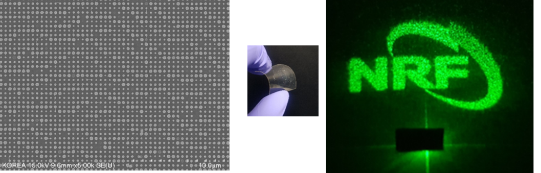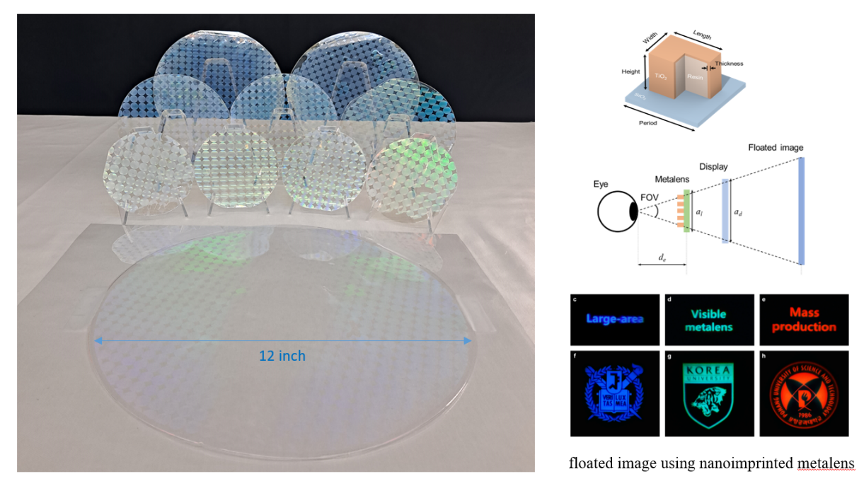
Figure. Nanoimprinted meta-surface and meta-hologram devices
Biography
Prof. Heon Lee receive his PhD degree from Stanford University in 1996. Then he worked for Bell Labs, Siemens Microelectronics and HP labs till 2003. After that, he joined Korea University, Department of Materials Science and Engineering as a faculty in 2004. His focused research area is nanoimprint lithography, radiative cooling and meta-surface. He is the author of 385 SCI papers with 11876 citations.
Eco-friendly Materials Design, Processing and Development for Future Ceramics Applications
Tohru Sekino
SANKEN, The University of Osaka, Ibaraki, Osaka 567-0047, Japan
sekino@sanken.osaka-u.ac.jp
Abstract
Eco-materials are attracting significant attention amid today's numerous environmental and energy challenges. The science and technology of eco-materials is expected not only endow the materials themselves with functions that reduce environmental impact such as catalysts for removing harmful substances or energy generation and storage capabilities but also to contribute to reducing energy consumption by utilizing low-environmental-impact processes in the fabrication of high-performance materials and devices. This paper overviews recent material developments achieved in ceramics and inorganic materials in our group. These achievements aim to solve various current challenges through advanced tuning of structures and functions coupled with novel process development and optimization
Various nanostructured oxides could be synthesized using solution chemical processes; Titania with nanotube structures (TNT) exhibited excellent photocatalytic and environmental purification properties due to the synergistic effects of its crystal structure, low-dimensional nanostructure, and the semiconductor and chemical properties of titania. While conventional methods for TNT synthesis required excessively high-concentration alkaline aqueous solutions, novel protocol using titanium peroxide complex solutions significantly reduced alkali consumption and enabled the peroxo groups modification to the TNTs. This allows the one-pot synthesis of visible-light-responsive peroxo-modified TNT (PTNT). This nano-titania responded to visible light and induced resultant charge separation and possessed photocatalytic performance capable of selectively cleaving specific chemical bonds of organic molecules. When attempting controlled hydrothermal synthesis, alkaline titanates were formed into a seaweed-like structure, and they exhibited excellent ion adsorption properties due to their layered structure, making them promising candidates for high-performance water purification materials.
On the other hand, fabricating bulk ceramics typically requires high-temperature sintering. Recently, however, cold sintering process (CSP) utilizing localized hydrothermal reactions between compacted ceramic particles have been attracting much attention. In this research, we report CSP and modified CSP methods based on low-temperature mineralization sintering protocol (LMSP) using reaction solutions containing constituent components for materials.
These methods allowed to promote dynamic dissolution and reprecipitation of inorganic phases such as nano-glass, calcium phosphates and non-oxide (silicon nitride) to densify nanosized raw materials. As a result, we successfully fabricated dense bulk ceramics at process temperatures below 300 °C. This paper outlines the fabrication of calcium phosphate-based sintered bodies (hydroxy apatite and whitlockite) and their structure and mechanical properties, which cannot be achieved by conventional sintering methods. Low-temperature densification of silicon nitride has been achieved by using surface pre-modified raw materials with silica phases. In addition, recent research achievements applying CSP to energy device materials, such as secondary battery electrodes, will also be discussed.
Biography
Professor Dr. Tohru Sekino graduated from Materials Chemistry at Tohoku University and obtained Ph.D. from Osaka University in 1997. He was recruited into Osaka University as a Research Associate in 1990, as an Associate Professor in 1999 at ISIR, and was appointed as an Assoc. Prof. at Tohoku University in 2007. He was then appointed as a full Professor at the Institute of Scientific and Industrial Research (SANKEN), Osaka University in 2014. Since April 2020 till March 2024, he served as the Director of SANKEN, Osaka University. He is involved in various cutting-edge investigations in design, development, function tuning and analysis coupled with novel process developments and optimizations for a wide variety of ceramics, ceramic-based nanocomposites, nanostructured and nanohybrid materials with multi-functions. Based on these material science and engineering research, he has published over 442 peer-reviewed publications in the worldwide scientific journals, which have been cited over 11,100 times (excluding self-cited papers), and invented more than 45 patents. Prof. Sekino received many awards including SPM Award for Distinguished Achievements in Research, Japan Society of Powder and Powder Metallurgy (May 2025), IUMRS Frontier Materials Scientists Awards (May 2022), The Ceramic Society of Japan Awards for Academic Achievements (May 2016), The Commendation for Science and Technology, the Minister of Education, Culture, Sports, Science and Technology (MEXT), Japan (April 2016), and so on.
The innovation-driven development of fluoride optical functional crystals: synthesis and applications pushing the limit
Liangbi Su
Shanghai Institute of Ceramics, Chinese Academy of Sciences
Email: suliangbi@mail.sic.ac.cn
Abstract
Optical functional crystals play an irreplaceable role in the development of laser technologies, semiconductor industries, high-end equipment manufacturing, etc. In the current era, the demands from both the scientific frontiers and the megaprojects are continuously driving the developments of optical functional crystals to overcome bottlenecks in the scaling of crystal sizes, the suppression of crystal defects and the improvement of the device performances. Such innovation-driven attempts are pushing the crystal growth and defect control of optical functional crystals towards the boundaries, in order to achieve ultra-large dimensions, ultra-low defects and extreme performances. Our research focuses on the design, crystal growth and characterizations of novel fluoride optical functional crystals for critical applications in fields such as lasers and high-precision optics: (1) We proposed the strategy of designing the luminescent behaviors of rare earth doped MF2 (M=Ca, Sr, Ba) crystals by tailoring the local coordinate structure via co-doping buffer ions. Special crystal lattice orders, i.e., “short-range disordered structures” embedded within the long-term periodic lattices, are created by manipulating the site environments of the rare earth dopants. A series of new laser crystals with performance exceeding that of traditional laser materials have been developed, establishing a new paradigm for the design of new laser crystals for diverse laser applications. (2) An in-situ observation method for real-time visualization of crystal growth interfaces was developed based on a conventional vertical Bridgman (VB) apparatus for fluoride crystal growth. The crucial bottlenecks of conventional crystal growth, i.e., the crystallization interfaces are neither detectable nor controllable, were overcome by establishing a feedback control system for maintaining stable solid-liquid (S-L) crystal growth interfaces with optimized shape, based on the capability to achieve quantitative information about the crystal growth processes by extracting the coordinates of S-L interfaces. Large-scale fluoride laser and optical crystals with high optical quality were successfully grown. (3) A series of breakthroughs in laser performances were achieved: in the ~1 μm spectral region, the laser pulse duration of solid-state laser based on Nd3+ doped fluoride crystals was suppressed to sub-100 fs range for the first time; in the ~2 μm spectral region, CW laser of a slope efficiency over 80% was realized using Tm:SrF2 crystals, corresponding to a quantum efficiency close to 200%; in the ~3 μm spectral region, high efficiency CW laser with the output power exceeding 15 watts was generated, which is to our best knowledge the highest record for CW mid-infrared lasers achieved in rare earth doped crystals. The outstanding laser performances indicate that these fluorite-type laser crystals are promising candidates for high-performance solid-state laser applications.
Biography
Dr. Liangbi Su is a professor from Shanghai Institute of Ceramics, Chinese Academy of Sciences (SICCAS). He is currently the director of SICCAS and also the director of the State Key Laboratory of Functional Crystals and Devices. He graduated from Wuhan University of Technology with a B.S and a M.S degree, and then received a doctoral degree from the Shanghai Institute of Optics and Fine Mechanics (SIOM), Chinese Academy of Sciences in 2005. He joined SICCAS in 2008 and is now leading “laser and optical crystals” research group, focusing on structure tailoring, crystal growth and characterization of fluoride crystals for laser and optical applications. He has published more than 300 scientific papers as the first or corresponding author and is the co-author of 6 books or titled book chapters. He has been granted 31 patents and has taken the lead in the establishment of 4 standards about fluoride crystals, including one recommended national standard. In 2014, Dr. Liangbi Su was awarded the Excellent Young Scientists Fund of NSFC. In 2019, he was awarded the National Science Fund for Distinguished Young Scholars. He is also the PI of the National Key R&D Program of China “Key Technologies of Crystal Growth and Applications of Large Size Laser Crystal Materials” as well as several other key research projects, including the CAS Project for Young Scientists in Basic Research.